
Differential Impedance Calculator
Review the pair cross-section before routing: compare width and edge gap, then keep the rest of the channel on the review list.
Design inputs
01 / CONFIGURECalculation workspace
02 / EXPLOREEstimate only for edge-coupled symmetric pairs. Not a solver for broadside pairs, asymmetric routing, discontinuities, connectors or reference-plane voids. Results are estimates; confirm critical designs with your fabricator.
How it works · formula & assumptions
Microstrip Zdiff ≈ 2Z0[1−0.48 exp(−0.96s/h)]. Symmetric stripline Zdiff ≈ 2Z0[1−0.347 exp(−2.9s/b)], b = 2h+t (coupling scale approximated as 2h).
Estimate only for edge-coupled symmetric pairs. Not a solver for broadside pairs, asymmetric routing, discontinuities, connectors or reference-plane voids.
Will the pair keep the same geometry through the route?
Will the pair keep the same geometry through the route?
A pair may begin with a sensible width and gap but change around a connector, pad escape or via field. Treat the calculator as a cross-section comparison; inspect the places where that cross-section stops being uniform.
Document geometry and channel requirements separately
For Circuit Edge layout work, define width, edge gap, reference layer and pair routing constraints in the board brief. Keep insertion loss, skew and connector transitions in a separate channel review. Matching a displayed differential impedance is not a complete interface validation.
The question this Circuit Edge workspace addresses
Review the pair cross-section before routing: compare width and edge gap, then keep the rest of the channel on the review list. Estimate only for edge-coupled symmetric pairs. Not a solver for broadside pairs, asymmetric routing, discontinuities, connectors or reference-plane voids.
Formula and assumptions
Microstrip Zdiff ≈ 2Z0[1−0.48 exp(−0.96s/h)]. Symmetric stripline Zdiff ≈ 2Z0[1−0.347 exp(−2.9s/b)], b = 2h+t (coupling scale approximated as 2h).
Distinguish differential and single-ended values
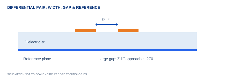
The single-ended reference describes the isolated conductor approximation. A nearby second trace changes odd-mode coupling, so the differential estimate is below the uncoupled twice-Z0 reference. As the edge-to-edge spacing grows, the estimate approaches that reference. Enter the copper edge gap rather than center-to-center pitch. A mistaken gap definition can produce a convincing number that describes a different geometry from the layout.
Keep the pair geometry consistent
This workspace considers edge-coupled microstrip or symmetric edge-coupled stripline with equal widths. It does not handle broadside pairs, different trace widths or asymmetric plane distances. The stripline coupling scale uses approximately twice the entered plane spacing and therefore omits a small thickness term in that coupling approximation. Confirm any selected differential width and gap using the fabricator field solver before applying a controlled-impedance tolerance.
Treat the channel as more than a cross-section
A target differential impedance does not by itself guarantee eye opening or protocol compliance. Connector launches, via stubs, return paths, insertion loss, skew and mode conversion all matter. Keep pair geometry consistent through bends and layer changes and avoid arbitrary spacing adjustments to repair length mismatch. When a pair crosses a plane split, the missing reference can dominate the channel behavior regardless of the nominal calculator result.
Use the estimate for sensitivity studies
Try a modest gap change while keeping width and stackup fixed, then observe the direction of the result. Repeat with realistic dielectric tolerance and finished width limits. These comparisons help frame a discussion with a fabricator; they do not produce a full statistical tolerance analysis. For USB, Ethernet, PCIe or other interfaces, obtain the actual target from the device and interface requirements and verify the complete channel with the appropriate analysis method.
Work from your project brief
Start by confirming the units shown beside each input. Enter the operating condition you expect in the finished product, then change one variable at a time so the effect stays clear. The plus and minus controls make small adjustments, while the slider is useful for a quick sensitivity sweep. Blank fields, impossible ranges and unsupported geometries stop the calculation instead of silently preserving a previous result. A unit change converts the displayed value while the underlying calculation keeps a consistent canonical unit system.
Keep a Circuit Edge board-review record
Use Copy Results for a design-review note, CSV for a calculation register, and Share Link to preserve the input values in the URL. Download PDF creates a local report with the inputs, outputs, formula and limitations. The exported estimate is only useful when its assumptions remain attached. Keep the board revision, stackup revision, supplier tolerances and applicable load or interface requirement in the same review record. A later fabrication change can invalidate an earlier calculation even if the calculator inputs have not changed.
Separate the displayed digits from project confidence
Several digits are displayed to make comparisons and unit conversions useful. Those digits do not imply matching physical accuracy. Manufacturing variation, environmental conditions and the simplicity of the selected model can dominate the final result. Round the chosen design requirement in a direction that preserves engineering margin, then agree the tolerance with your fabricator. Use prototype measurements and the relevant analysis tools when a small change would affect reliability, regulatory compliance or product performance.
Worked example
For the default microstrip geometry, the coupled differential estimate is below the uncoupled 2Z0 reference. Increasing the gap makes it approach 2Z0. Use the defaults as a reproducible starting point, then substitute your own board data. When comparing a manual calculation, keep dimensional units consistent and avoid rounding intermediate values. If your result differs, check the input definitions before changing the model or applying an unexplained correction factor.
Continue with our calculation methodology, fabrication review checklist and high-speed layout guide. For board-specific support, contact Circuit Edge Technologies.
Frequently asked questions
What does the differential impedance tool calculate?
Review the pair cross-section before routing: compare width and edge gap, then keep the rest of the channel on the review list. Estimate only for edge-coupled symmetric pairs. Not a solver for broadside pairs, asymmetric routing, discontinuities, connectors or reference-plane voids.
Which formula does this calculator use?
Microstrip Zdiff ≈ 2Z0[1−0.48 exp(−0.96s/h)]. Symmetric stripline Zdiff ≈ 2Z0[1−0.347 exp(−2.9s/b)], b = 2h+t (coupling scale approximated as 2h). The Methodology page records the model and its limitations so that a design reviewer can reproduce the assumptions.
How should I check the input definitions?
The single-ended reference describes the isolated conductor approximation. A nearby second trace changes odd-mode coupling, so the differential estimate is below the uncoupled twice-Z0 reference. As the edge-to-edge spacing grows, the estimate approaches that reference. Enter the copper edge gap rather than center-to-center pitch. A mistaken gap definition can produce a convincing number that describes a different geometry from the layout.
What is a useful worked example?
For the default microstrip geometry, the coupled differential estimate is below the uncoupled 2Z0 reference. Increasing the gap makes it approach 2Z0. This example is a starting point for checking units, not a universal production recommendation.
Can I use the result as a fabrication or compliance approval?
Estimate only for edge-coupled symmetric pairs. Not a solver for broadside pairs, asymmetric routing, discontinuities, connectors or reference-plane voids. Obtain the required engineering and manufacturing review before releasing a critical design.
How can I save and share my calculation?
Copy Results includes the inputs, outputs and limitations. CSV provides a local record, while Download PDF creates a local engineering report. Share Link encodes the canonical input values in the URL. Anyone with the link can reproduce that input set.
What should I verify before design release?
Try a modest gap change while keeping width and stackup fixed, then observe the direction of the result. Repeat with realistic dielectric tolerance and finished width limits. These comparisons help frame a discussion with a fabricator; they do not produce a full statistical tolerance analysis. For USB, Ethernet, PCIe or other interfaces, obtain the actual target from the device and interface requirements and verify the complete channel with the appropriate analysis method.
Inputs and related calculators
Transmission line, Relative permittivity, Trace to nearest plane, Trace width, Copper thickness, Edge-to-edge pair gap.