
PCB Thermal Relief Calculator
Review the pad-to-plane connection as both an electrical path and an assembly decision, using an ideal copper-spoke comparison.
Design inputs
01 / CONFIGURECalculation workspace
02 / EXPLOREOne-dimensional copper conduction only. Not a pad temperature, solderability, thermal-via or board-to-ambient thermal model. Spoke spreading and contact effects are omitted. Results are estimates; confirm critical designs with your fabricator.
How it works · formula & assumptions
A_total = Nwt; R_electrical = ρL/A_total; R_thermal = L/(κA_total), κ = 401 W/(m·K), ρ = 1.724×10⁻⁸ Ω·m at 20 °C.
One-dimensional copper conduction only. Not a pad temperature, solderability, thermal-via or board-to-ambient thermal model. Spoke spreading and contact effects are omitted.
Will the pad connection work electrically and assemble cleanly?
Will the pad connection work electrically and assemble cleanly?
A solid pour can improve conduction while making a through-hole terminal harder to solder. A relief that improves soldering may become the narrowest section of a power path. Discuss both objectives before choosing the spoke rule.
Check the copper after the final refill
The Circuit Edge manufacturing review should count actual spokes in the released copper, not merely in a CAD rule dialog. Compare their total section with the connected trace and barrel. Confirm the intended soldering and rework process with assembly before calling the connection complete.
The question this Circuit Edge workspace addresses
Review the pad-to-plane connection as both an electrical path and an assembly decision, using an ideal copper-spoke comparison. One-dimensional copper conduction only. Not a pad temperature, solderability, thermal-via or board-to-ambient thermal model. Spoke spreading and contact effects are omitted.
Formula and assumptions
A_total = Nwt; R_electrical = ρL/A_total; R_thermal = L/(κA_total), κ = 401 W/(m·K), ρ = 1.724×10⁻⁸ Ω·m at 20 °C.
Define the modeled path
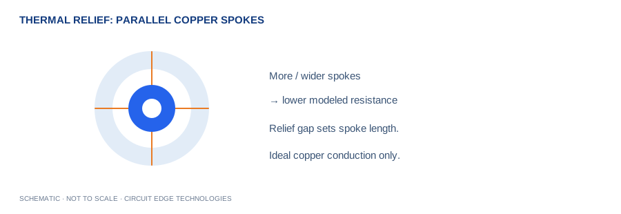
The relief gap is treated as the straight length of each copper spoke between the pad and surrounding copper. Every spoke has the same width and thickness. Their cross-sections are summed as parallel conduction paths. This is a deliberately simple one-dimensional model. Rounded junctions, spoke taper, spreading resistance in the pad and plane, and nearby copper clearances can make the real structure depart substantially from this idealization.
Separate electrical and thermal resistance
Electrical resistance describes voltage drop per ampere through the copper at the assumed reference temperature. Thermal resistance describes the ideal temperature difference per watt along the same copper path. These quantities use different material properties and cannot be substituted for one another. The reported K/W number does not include convection, board dielectric or component junction resistance and therefore is not a board-to-ambient thermal rating.
Balance solderability against conduction
Wider or more numerous spokes reduce modeled resistance, but they also connect the pad more strongly to surrounding copper during soldering. A solid plane attachment may make hand soldering or rework more difficult. The correct relief depends on assembly process, copper weight, component type and required load current. Ask the assembler to review the chosen geometry rather than assuming that the lowest electrical resistance always produces the best manufacturing outcome.
Validate local bottlenecks
Compare spoke cross-section with the connected trace, barrel and component terminal. A generous plane does not compensate for a narrow relief that concentrates current. Verify that actual CAD connectivity produces the intended number of spokes after copper refill and clearance enforcement. Inspect the final fabrication outputs, not just the nominal pad rule. If a high-current connection needs solid attachment, document how the assembly process will manage the additional thermal mass.
Work from your project brief
Start by confirming the units shown beside each input. Enter the operating condition you expect in the finished product, then change one variable at a time so the effect stays clear. The plus and minus controls make small adjustments, while the slider is useful for a quick sensitivity sweep. Blank fields, impossible ranges and unsupported geometries stop the calculation instead of silently preserving a previous result. A unit change converts the displayed value while the underlying calculation keeps a consistent canonical unit system.
Keep a Circuit Edge board-review record
Use Copy Results for a design-review note, CSV for a calculation register, and Share Link to preserve the input values in the URL. Download PDF creates a local report with the inputs, outputs, formula and limitations. The exported estimate is only useful when its assumptions remain attached. Keep the board revision, stackup revision, supplier tolerances and applicable load or interface requirement in the same review record. A later fabrication change can invalidate an earlier calculation even if the calculator inputs have not changed.
Separate the displayed digits from project confidence
Several digits are displayed to make comparisons and unit conversions useful. Those digits do not imply matching physical accuracy. Manufacturing variation, environmental conditions and the simplicity of the selected model can dominate the final result. Round the chosen design requirement in a direction that preserves engineering margin, then agree the tolerance with your fabricator. Use prototype measurements and the relevant analysis tools when a small change would affect reliability, regulatory compliance or product performance.
Worked example
Four 0.30 mm wide, 35 µm thick spokes across 0.25 mm give about 0.103 mΩ electrical resistance and 14.84 K/W ideal copper conduction resistance. Use the defaults as a reproducible starting point, then substitute your own board data. When comparing a manual calculation, keep dimensional units consistent and avoid rounding intermediate values. If your result differs, check the input definitions before changing the model or applying an unexplained correction factor.
Continue with our calculation methodology, fabrication review checklist and high-speed layout guide. For board-specific support, contact Circuit Edge Technologies.
Frequently asked questions
What does the thermal relief tool calculate?
Review the pad-to-plane connection as both an electrical path and an assembly decision, using an ideal copper-spoke comparison. One-dimensional copper conduction only. Not a pad temperature, solderability, thermal-via or board-to-ambient thermal model. Spoke spreading and contact effects are omitted.
Which formula does this calculator use?
A_total = Nwt; R_electrical = ρL/A_total; R_thermal = L/(κA_total), κ = 401 W/(m·K), ρ = 1.724×10⁻⁸ Ω·m at 20 °C. The Methodology page records the model and its limitations so that a design reviewer can reproduce the assumptions.
How should I check the input definitions?
The relief gap is treated as the straight length of each copper spoke between the pad and surrounding copper. Every spoke has the same width and thickness. Their cross-sections are summed as parallel conduction paths. This is a deliberately simple one-dimensional model. Rounded junctions, spoke taper, spreading resistance in the pad and plane, and nearby copper clearances can make the real structure depart substantially from this idealization.
What is a useful worked example?
Four 0.30 mm wide, 35 µm thick spokes across 0.25 mm give about 0.103 mΩ electrical resistance and 14.84 K/W ideal copper conduction resistance. This example is a starting point for checking units, not a universal production recommendation.
Can I use the result as a fabrication or compliance approval?
One-dimensional copper conduction only. Not a pad temperature, solderability, thermal-via or board-to-ambient thermal model. Spoke spreading and contact effects are omitted. Obtain the required engineering and manufacturing review before releasing a critical design.
How can I save and share my calculation?
Copy Results includes the inputs, outputs and limitations. CSV provides a local record, while Download PDF creates a local engineering report. Share Link encodes the canonical input values in the URL. Anyone with the link can reproduce that input set.
What should I verify before design release?
Compare spoke cross-section with the connected trace, barrel and component terminal. A generous plane does not compensate for a narrow relief that concentrates current. Verify that actual CAD connectivity produces the intended number of spokes after copper refill and clearance enforcement. Inspect the final fabrication outputs, not just the nominal pad rule. If a high-current connection needs solid attachment, document how the assembly process will manage the additional thermal mass.
Inputs and related calculators
Spoke width, Number of spokes, Spoke length / relief gap, Copper thickness.