
Eagle PCB Trace Width Review Workflow
Review a Circuit Edge power path: compare minimum copper width, resistive loss and the allowance you will carry into layout.
Eagle PCB Trace Width Review Workflow
This example begins at 1.5 amperes on one-ounce outer copper. Use your project data before applying a width rule in the installed Eagle environment. The calculator provides geometry and electrical estimates; it does not import the board or synchronize the rule settings. Review the actual tool documentation for the version used by your team.
Design inputs
01 / CONFIGURECalculation workspace
02 / EXPLOREThis legacy IPC-2221 power law is an early sizing model, not an IPC-2152 thermal simulation. Nearby copper, enclosure, airflow and neck-downs change actual heating. Results are estimates; confirm critical designs with your fabricator.
How it works · formula & assumptions
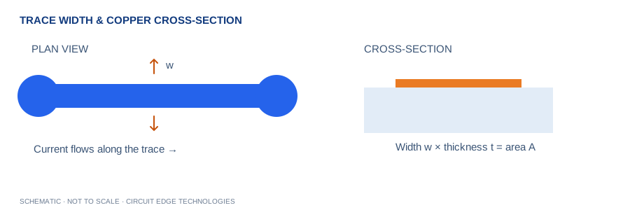
I = k × ΔT^0.44 × A^0.725; w = A / t. k = 0.048 external or 0.024 internal; A and t in mil units.
This legacy IPC-2221 power law is an early sizing model, not an IPC-2152 thermal simulation. Nearby copper, enclosure, airflow and neck-downs change actual heating.
Connect electrical assumptions with layout constraints
This example begins at 1.5 amperes on one-ounce outer copper. Use your project data before applying a width rule in the installed Eagle environment. The calculator provides geometry and electrical estimates; it does not import the board or synchronize the rule settings. Review the actual tool documentation for the version used by your team.
Review priorities for this case
Check polygons and isolated neck-downs after copper processing, then compare the feeding trace with pad and via geometry. Keep a copy of the original constraint decision and verify that later rerouting did not reduce the narrowest part of the path. Manufacturing output review remains necessary after a clean CAD check.
Model and limits
I = k × ΔT^0.44 × A^0.725; w = A / t. k = 0.048 external or 0.024 internal; A and t in mil units.
This legacy IPC-2221 power law is an early sizing model, not an IPC-2152 thermal simulation. Nearby copper, enclosure, airflow and neck-downs change actual heating.
Compare before committing
Change one assumption at a time and save the resulting input set with the board revision. Compare the estimate with the full tool explanation, then check local bottlenecks and manufacturing tolerances. These case values describe one starting scenario; they do not replace the product requirements or the fabricator stackup.
Continue with our calculation methodology, fabrication review checklist and high-speed layout guide. For board-specific support, contact Circuit Edge Technologies.
Frequently asked questions
What does the trace width tool calculate?
Review a Circuit Edge power path: compare minimum copper width, resistive loss and the allowance you will carry into layout. This legacy IPC-2221 power law is an early sizing model, not an IPC-2152 thermal simulation. Nearby copper, enclosure, airflow and neck-downs change actual heating.
Which formula does this calculator use?
I = k × ΔT^0.44 × A^0.725; w = A / t. k = 0.048 external or 0.024 internal; A and t in mil units. The Methodology page records the model and its limitations so that a design reviewer can reproduce the assumptions.
How should I check the input definitions?
Temperature rise is an increase above the local ambient, not the absolute copper temperature. A board in a sealed enclosure may already be substantially warmer than the room. Enter the ambient near the conductor and decide how much extra heating the surrounding components can tolerate. The resistance calculation uses ambient plus the selected rise, referenced to copper resistivity at 20 °C. This is an assumed operating temperature, not a solved thermal equilibrium.
What is a useful worked example?
At 1 A, 10 °C rise and 1 oz external copper, the required width is approximately 0.301 mm. A 15% margin raises this to approximately 0.346 mm. This example is a starting point for checking units, not a universal production recommendation.
Can I use the result as a fabrication or compliance approval?
This legacy IPC-2221 power law is an early sizing model, not an IPC-2152 thermal simulation. Nearby copper, enclosure, airflow and neck-downs change actual heating. Obtain the required engineering and manufacturing review before releasing a critical design.
How can I save and share my calculation?
Copy Results includes the inputs, outputs and limitations. CSV provides a local record, while Download PDF creates a local engineering report. Share Link encodes the canonical input values in the URL. Anyone with the link can reproduce that input set.
What should I verify before design release?
Record the calculated minimum and the chosen design width as separate values. Round upward to a sensible CAD rule, then inspect the entire path at that rule. For short pulses, model the waveform and transient heating instead of entering a peak value as if it were continuous current. For sustained high power, evaluate planes, busbars, copper inserts or alternative layer allocation. Measure the prototype at the expected enclosure temperature and airflow.