
FR4 PCB Impedance Stackup Review
Bring a proposed stackup to the Circuit Edge design desk and examine how its width and reference spacing affect the estimate.
FR4 PCB Impedance Stackup Review
The default εr of 4.2 is illustrative and should be replaced with data for the actual laminate, glass construction and frequency. Resin distribution and pressed dielectric thickness influence the field around a trace. Begin with the board supplier stackup and use this tool to understand whether a proposed width change moves the impedance in the intended direction.
Design inputs
01 / CONFIGURECalculation workspace
02 / EXPLOREEstimate only. Simple closed-form formulas omit solder mask, trapezoidal etching, copper roughness, frequency dispersion and nearby conductors. Symmetric stripline only; h is the copper-surface distance to either plane. Results are estimates; confirm critical designs with your fabricator.
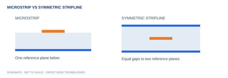
How it works · formula & assumptions
Microstrip Z0 = 87/√(εr+1.41) × ln[5.98h/(0.8w+t)]. Symmetric stripline Z0 = 60/√εr × ln[1.9b/(0.8w+t)], b = 2h+t.
Estimate only. Simple closed-form formulas omit solder mask, trapezoidal etching, copper roughness, frequency dispersion and nearby conductors. Symmetric stripline only; h is the copper-surface distance to either plane.
FR4 is a material family, not one dielectric number
The default εr of 4.2 is illustrative and should be replaced with data for the actual laminate, glass construction and frequency. Resin distribution and pressed dielectric thickness influence the field around a trace. Begin with the board supplier stackup and use this tool to understand whether a proposed width change moves the impedance in the intended direction.
Review priorities for this case
Ask the supplier to confirm final controlled-impedance dimensions and coupon testing. The simple formula omits solder mask and etch profile. For fast interfaces or tight tolerances, use a suitable field solver and include losses and discontinuities in the channel review.
Model and limits
Microstrip Z0 = 87/√(εr+1.41) × ln[5.98h/(0.8w+t)]. Symmetric stripline Z0 = 60/√εr × ln[1.9b/(0.8w+t)], b = 2h+t.
Estimate only. Simple closed-form formulas omit solder mask, trapezoidal etching, copper roughness, frequency dispersion and nearby conductors. Symmetric stripline only; h is the copper-surface distance to either plane.
Compare before committing
Change one assumption at a time and save the resulting input set with the board revision. Compare the estimate with the full tool explanation, then check local bottlenecks and manufacturing tolerances. These case values describe one starting scenario; they do not replace the product requirements or the fabricator stackup.
Continue with our calculation methodology, fabrication review checklist and high-speed layout guide. For board-specific support, contact Circuit Edge Technologies.
Frequently asked questions
What does the single-ended impedance tool calculate?
Bring a proposed stackup to the Circuit Edge design desk and examine how its width and reference spacing affect the estimate. Estimate only. Simple closed-form formulas omit solder mask, trapezoidal etching, copper roughness, frequency dispersion and nearby conductors. Symmetric stripline only; h is the copper-surface distance to either plane.
Which formula does this calculator use?
Microstrip Z0 = 87/√(εr+1.41) × ln[5.98h/(0.8w+t)]. Symmetric stripline Z0 = 60/√εr × ln[1.9b/(0.8w+t)], b = 2h+t. The Methodology page records the model and its limitations so that a design reviewer can reproduce the assumptions.
How should I check the input definitions?
Impedance is a property of the conductor and its surrounding electromagnetic geometry. A width without a reference-plane distance is not enough. For microstrip, h is the dielectric distance from the conductor underside to the reference plane. For this symmetric stripline approximation, h is the equal surface-to-plane spacing on each side, so the plane separation is twice h plus copper thickness. Asymmetric constructions require a different model.
What is a useful worked example?
For microstrip with εr 4.2, h 0.18 mm, w 0.30 mm and t 35 µm, Z0 is approximately 50 Ω. This example is a starting point for checking units, not a universal production recommendation.
Can I use the result as a fabrication or compliance approval?
Estimate only. Simple closed-form formulas omit solder mask, trapezoidal etching, copper roughness, frequency dispersion and nearby conductors. Symmetric stripline only; h is the copper-surface distance to either plane. Obtain the required engineering and manufacturing review before releasing a critical design.
How can I save and share my calculation?
Copy Results includes the inputs, outputs and limitations. CSV provides a local record, while Download PDF creates a local engineering report. Share Link encodes the canonical input values in the URL. Anyone with the link can reproduce that input set.
What should I verify before design release?
Use this workspace to explore direction and sensitivity: wider traces generally lower impedance, while a more distant plane generally raises it. Then send a target impedance and tolerance to the board supplier and agree on the final width and coupon strategy. Review reference-plane continuity and transitions independently; a uniform-line estimate cannot certify an entire channel. Read the existing microstrip article for layout context and include an impedance report with the release package.