
0.3 mm Via Current Estimate for Two Vias
Examine a layer transition before the PCB release: barrel geometry, array resistance and the limits of a shared-current assumption.
0.3 mm Via Current Estimate for Two Vias
Two small plated through vias are a common way to connect a local supply region to another layer. This preset uses a 0.30 mm finished hole, 25 µm barrel plating and 1.6 mm conductor length. It assumes both barrels have identical resistance and receive current equally. The electrical resistance estimate is more directly tied to geometry than the thermal current screening value; the latter maps a trace law onto a cylindrical conductor and needs independent validation.
Design inputs
01 / CONFIGURECalculation workspace
02 / EXPLOREMapping the trace power law to barrel area is a heuristic, not a validated IPC via rating. Linear current scaling assumes identical, equally fed vias; mutual heating and unequal sharing are omitted. Results are estimates; confirm critical designs with your fabricator.
How it works · formula & assumptions
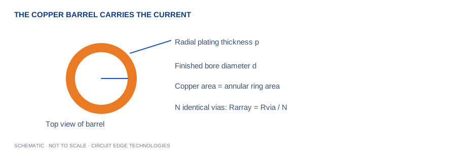
A = π[(d/2+p)² − (d/2)²]; R = ρL/A; array R = R/N. Screening I = N × 0.024 × ΔT^0.44 × A_mil²^0.725.
Mapping the trace power law to barrel area is a heuristic, not a validated IPC via rating. Linear current scaling assumes identical, equally fed vias; mutual heating and unequal sharing are omitted.
A compact two-via layer transition
Two small plated through vias are a common way to connect a local supply region to another layer. This preset uses a 0.30 mm finished hole, 25 µm barrel plating and 1.6 mm conductor length. It assumes both barrels have identical resistance and receive current equally. The electrical resistance estimate is more directly tied to geometry than the thermal current screening value; the latter maps a trace law onto a cylindrical conductor and needs independent validation.
Review priorities for this case
Keep the feeds broad and symmetrical. Two vias placed in series along a narrow incoming trace may not share current as evenly as two equally fed branches. Inspect the copper annulus and internal-plane connection, then compare this transition with the feeding trace and any thermal spokes.
Model and limits
A = π[(d/2+p)² − (d/2)²]; R = ρL/A; array R = R/N. Screening I = N × 0.024 × ΔT^0.44 × A_mil²^0.725.
Mapping the trace power law to barrel area is a heuristic, not a validated IPC via rating. Linear current scaling assumes identical, equally fed vias; mutual heating and unequal sharing are omitted.
Compare before committing
Change one assumption at a time and save the resulting input set with the board revision. Compare the estimate with the full tool explanation, then check local bottlenecks and manufacturing tolerances. These case values describe one starting scenario; they do not replace the product requirements or the fabricator stackup.
Continue with our calculation methodology, fabrication review checklist and high-speed layout guide. For board-specific support, contact Circuit Edge Technologies.
Frequently asked questions
What does the via current tool calculate?
Examine a layer transition before the PCB release: barrel geometry, array resistance and the limits of a shared-current assumption. Mapping the trace power law to barrel area is a heuristic, not a validated IPC via rating. Linear current scaling assumes identical, equally fed vias; mutual heating and unequal sharing are omitted.
Which formula does this calculator use?
A = π[(d/2+p)² − (d/2)²]; R = ρL/A; array R = R/N. Screening I = N × 0.024 × ΔT^0.44 × A_mil²^0.725. The Methodology page records the model and its limitations so that a design reviewer can reproduce the assumptions.
How should I check the input definitions?
The finished hole is the empty bore after plating. Copper occupies a ring around that bore; its cross-section is not the circular hole area. The calculator uses finished hole diameter and radial wall plating to compute the copper annulus. If your fabricator supplies drill diameter instead, obtain the finished-hole target before using this model. Plating thickness on an outer surface is not necessarily the same as the guaranteed minimum inside the hole.
What is a useful worked example?
A 0.30 mm finished hole with 25 µm radial plating contains about 0.0255 mm² of barrel copper. Two identical 1.6 mm barrels have about 0.54 mΩ resistance at 20 °C. This example is a starting point for checking units, not a universal production recommendation.
Can I use the result as a fabrication or compliance approval?
Mapping the trace power law to barrel area is a heuristic, not a validated IPC via rating. Linear current scaling assumes identical, equally fed vias; mutual heating and unequal sharing are omitted. Obtain the required engineering and manufacturing review before releasing a critical design.
How can I save and share my calculation?
Copy Results includes the inputs, outputs and limitations. CSV provides a local record, while Download PDF creates a local engineering report. Share Link encodes the canonical input values in the URL. Anyone with the link can reproduce that input set.
What should I verify before design release?
Specify minimum barrel plating, aspect ratio and reliability requirements in the fabrication package. Use short, broad feed regions on every connected layer. Check pad and antipad geometry so nearby clearances do not create a bottleneck. Compare the via array with the trace feeding it and inspect the return connection. On a prototype, measure temperature near the transition under continuous load and verify that connector or pad resistance is not dominating the result.